
With the significance of semiconductors solely growing throughout a number of industries, a brand new facility in Scotland may assist bolster the worth chain within the essential side of packaging.
Demand for superior semiconductor packaging is rising quickly in parallel with the event of next-generation applied sciences, together with synthetic intelligence (AI), photonics, quantum, and built-in sensing techniques. The complexity of gadgets heightens the significance of superior packaging for demanding purposes.

Entry deeper trade intelligence
Expertise unmatched readability with a single platform that mixes distinctive knowledge, AI, and human experience.
“Semiconductor packaging is now not seen as a passive safety mechanism,” says Dr Gladys Benghalia, head of programmes in electrification manufacturing on the Nationwide Manufacturing Institute Scotland (NMIS). “It has developed into an enabling platform – the convergence level for a number of superior applied sciences. We’re seeing the combination of supplies, design and performance, the place the bundle defines the system-level structure. It’s inside the packaging area that we are able to now engineer efficiency, energy effectivity, thermal administration and price trade-offs on the machine stage.”
The worldwide development of superior semiconductor packaging
In an ever-more related world, myriad applied sciences depend on semiconductors. By 2029, GlobalData predicts the worldwide semiconductors market will likely be price $993.3bn, rising by 63.2% from 2024. By 2030, the worldwide market worth may simply prime $1trn.
The worldwide semiconductor manufacturing market is dominated by the Asia-Pacific, which had a 74.4% share in 2024. Inside this, China and Taiwan are each distinguished manufacturing places.
Nevertheless, the three-year scarcity of semiconductors from 2020-23 uncovered the issues in present provide chains being over-reliant on too few places. Alongside this, geopolitical tensions and provide chain disruptions of latest years have pressured nations to concentrate on extra resilient home manufacturing capabilities.
Moreover, sooner innovation is required for semiconductor packaging capabilities to maintain up with specialist calls for. Assembly complicated necessities may be difficult for the high-volume manufacturing fashions prevalent throughout South East Asia. If semiconductor packaging strains are unable to supply superior options for next-generation applied sciences, the innovation curve will likely be restricted, and alternatives to develop important options will likely be missed.
The UK is well-positioned to develop such capabilities and contribute to the worldwide worth chain, eradicating the reliance on worldwide suppliers for key elements. UK semiconductor packaging is rising at a compound annual development charge of virtually 11%. According to this development, the worldwide packaging market can also be increasing.
For semiconductors, the packaging is a vital side that goes far past mere encapsulation and Scotland is growing specialist capabilities on this important space.
“We’re growing packaging options that actively outline system behaviour, slightly than simply merely housing chips,” provides Benghalia.
Superior semiconductor packaging facility in Europe
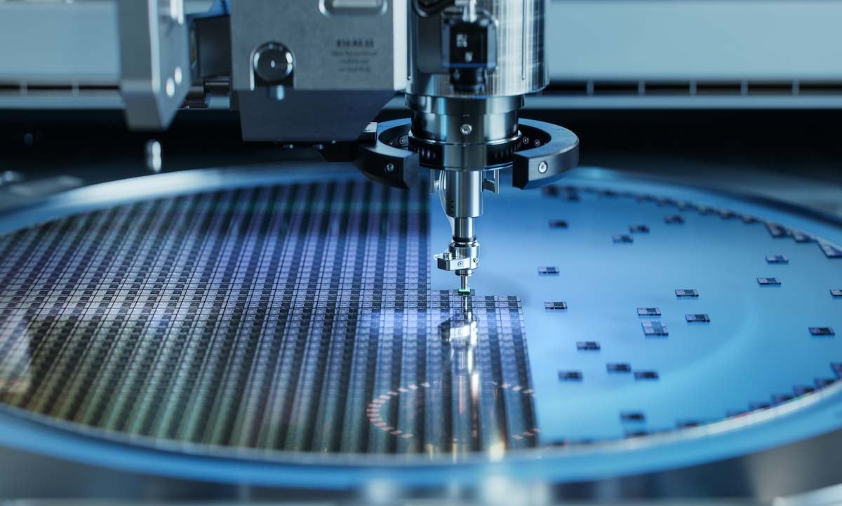
On the forefront of tech innovation in Scotland is the Nationwide Superior Semiconductor Packaging and Integration Centre (NASPIC), which was formally introduced in July and is a key facility in assembly elevated demand. Primarily based close to Glasgow Airport, NASPIC is the primary open-access facility of its variety in Europe and can help accelerated improvement timelines of semiconductors, offering packaging in a matter of days as a substitute of months.
The Nationwide Manufacturing Institute Scotland (NMIS) is the driving pressure behind NASPIC, which will likely be integral to the Superior Web Zero Innovation Centre (ANZIC) on the College of Strathclyde. Over the subsequent decade, NASPIC is projected to allow £800m in income for UK and worldwide companies and help 300 jobs.

NASPIC is a nationwide hub for superior semiconductor packaging improvement, benefiting from a portion of the £160m funding from the UK Authorities throughout initiatives within the Glasgow Metropolis Area Innovation Zone (GCRIZ).
NASPIC obtained an £8m grant from Innovate UK’s Driving the Electrical Revolution (DER) Problem, alongside funding from Scottish Enterprise, for superior packaging in energy electronics. To additional capabilities, GCRIZ and Scottish Enterprise are planning to speculate an extra £29m to develop the modern services into photonics, RF, quantum computing and high-performance compute/AI constructed on superior CMOS applied sciences.
The brand new facility can have the capability to help each UK and world clients, providing lab-to-line superior semiconductor packaging elements for vital purposes.
Whereas NASPIC can’t compete with the main producers of South East Asia when it comes to quantity, the Scottish website has an edge in offering high-value sovereign meeting prototyping.
“At NASPIC, we’re accelerating the prototyping and scale-up of superior packaging assemblies so innovation can circulation quickly into manufacturing in an trade that’s evolving at extraordinary velocity,” saysBenghalia.
UK semiconductor packaging capabilities
UK wafer fabs sometimes use offshore suppliers of semiconductor packaging, which might delay improvement timelines by months and expose producers to provide chain disruption.
Manufacturing within the UK will help home manufacturing and assist to raised insulate in opposition to provide chain disruption and geopolitical occasions. Past Scotland, the power gives worldwide semiconductor firms the chance to develop low-volume, high-value options for complicated tech wants which are solely attainable in a couple of places globally.
State-of-the-art tools at NASPIC will present companions with full functionality throughout the superior packaging workflow, from wafer preparation, dicing and die connect, via interconnect, encapsulation and meeting, to subsystem integration and testing.
“Our method permits firms to really perceive how their expertise will scale, not simply whether or not it really works in precept,” provides Benghalia. “It’s a particular energy of the College of Strathclyde and NMIS: integrating analysis, improvement and manufacturing functionality, giving our companions the arrogance to scale new applied sciences into real-world purposes.”
The pilot manufacturing atmosphere permits companions to show and qualify packaging throughout areas corresponding to energy electronics, photonics, radio frequency (RF), superior complementary metal-oxide-semiconductor (CMOS), and high-performance computing.
NASPIC has additionally attracted curiosity from producers in South East Asia because of the capability for analysis and innovation that isn’t as distinguished in high-volume manufacturing places.
“We’re not doing analysis that merely advances information, we’re closing the hole between innovation and industrial adoption, guaranteeing new applied sciences can transfer confidently from the lab to line,” says Benghalia.
The ambition of Scotland in vital applied sciences
The long-term ambition behind the power is to ascertain Glasgow as a recognised centre of excellence within the ultra-specialist discipline of superior semiconductor packaging. Collaborations are on the centre of Scottish improvements at NASPIC, established in partnership with the Compound Semiconductor Functions (CSA) Catapult, whereas complementing capabilities at James Watt Nanofabrication Centre (JWNC), which might produce sensors, lasers and qubits, for instance, for integration into the packages.
The services and partnerships are integral to Scotland’s development technique in its Vital Applied sciences Supercluster, connecting the nation’s world-class universities with companies and authorities.
“Scotland’s ecosystem is extremely wealthy, and the Vital Applied sciences Supercluster is an ideal instance. It connects our nationwide strengths in photonics, quantum, semiconductors and sensing and connectivity, bringing collectively over 150 firms to speed up cross-sector innovation and industrial development,” provides Benghalia.
The supercluster was introduced in November 2024, with the applied sciences within the 4 areas estimated to be price £4.2bn in gross sales.
With its foundations in analysis, the ambition for the supercluster is anticipated to attain a mixed turnover of £10bn by 2035 and is projected to outcome within the creation of 6,600 extra expert jobs.
There are notable crossovers between the 4 pillars of the Vital Applied sciences Supercluster, which has been established to foster collaboration, increase funding, and develop expertise of the growing workforce. These components all place Scotland strongly to attain future development in vital applied sciences and optimise market alternatives within the tech economic system.
To study extra concerning the improvement of Scotland’s Vital Applied sciences Supercluster, obtain the doc under.

Join our each day information round-up!
Give your small business an edge with our main trade insights.