
Siemens and GlobalFoundries (GF) have introduced a brand new partnership to combine AI-driven applied sciences into semiconductor manufacturing, focusing on elevated effectivity and reliability throughout manufacturing processes.
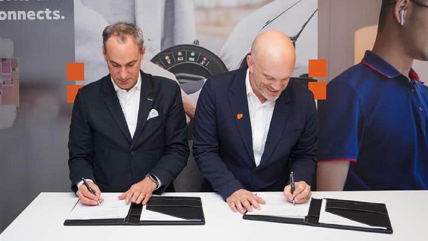
The collaboration, formalised via a memorandum of understanding (MoU), spans areas comparable to fab automation, electrification, and the deployment of digital options all through the semiconductor lifecycle.

Entry deeper business intelligence
Expertise unmatched readability with a single platform that mixes distinctive knowledge, AI, and human experience.
The businesses will concentrate on implementing superior AI-enabled software program, sensors, and real-time management methods inside semiconductor fabrication environments.
By centralised automation and predictive upkeep, Siemens and GF plan to lift gear availability and streamline chip manufacturing workflows.
Each organisations intend to pilot these options in their very own manufacturing operations with the potential to increase profitable approaches into different superior expertise sectors.
In keeping with the events, this settlement comes as demand surges for semiconductors in important domains together with AI, defence, power infrastructure, and world connectivity platforms.
By combining experience, Siemens and GF search to deal with business necessities for safe and dependable provide chains whereas aiming to boost industrial resilience via automation.
Siemens brings to the desk its suite of applied sciences for industrial, power, and constructing automation, alongside software program for chip design, manufacturing course of administration, fab automation, and product lifecycle administration. These capabilities are anticipated to assist seamless integration throughout a number of phases of semiconductor manufacturing and supply.
Siemens managing board member and digital industries CEO Cedrik Neike mentioned: “Our economic system runs on Silicon – one wafer at a time. Chips are important for purposes like robotics or connectivity and for bringing AI into the bodily world and business.
“We’re collaborating to make world semiconductor provide chains extra resilient and to allow environment friendly localised manufacturing world wide.”
The Siemens-GF partnership is structured to permit each corporations to leverage these instruments in growing and manufacturing high-performance chips at scale.
GF contributes specialised course of expertise and design experience via its foundry operations in addition to via MIPS, its subsidiary targeted on RISC-V processor IP.
Along with Siemens’ applied sciences, this experience shall be utilized to speed up improvement cycles for customized semiconductor options tailor-made to purposes comparable to autonomous methods and AI {hardware} platforms.
GF’s operational footprint contains manufacturing amenities throughout the US, Asia, and Europe. Its Dresden web site stays the most important semiconductor manufacturing facility in Europe with roughly 3,000 staff.
GF CEO Tim Breen mentioned: “Safe, regionally manufactured semiconductors are on the core of the AI transition – from cloud to the bodily world, bringing intelligence into gadgets we use daily and enabling purposes we couldn’t think about a number of years in the past.
“Our distinctive collaboration with Siemens permits us to go sooner – to construct the applied sciences that make this attainable – differentiated, energy-efficient, linked and safe chips throughout a variety of next-generation purposes.”
In November 2025, GF entered right into a separate long-term partnership with Navitas Semiconductor aimed toward advancing gallium nitride (GaN) expertise within the US.
The settlement covers the co-development and supply of options for high-power purposes together with datacentres, high-performance computing infrastructure, grid methods, and industrial electrification initiatives. The transfer is designed to bolster home GaN provide chains whereas supporting decarbonisation goals in rising power and compute markets.

Join our each day information round-up!
Give what you are promoting an edge with our main business insights.